// The systems read, in writing
The Invisible Geometry: How Sony Won the Smartphone War by Redesigning the Floor Plan
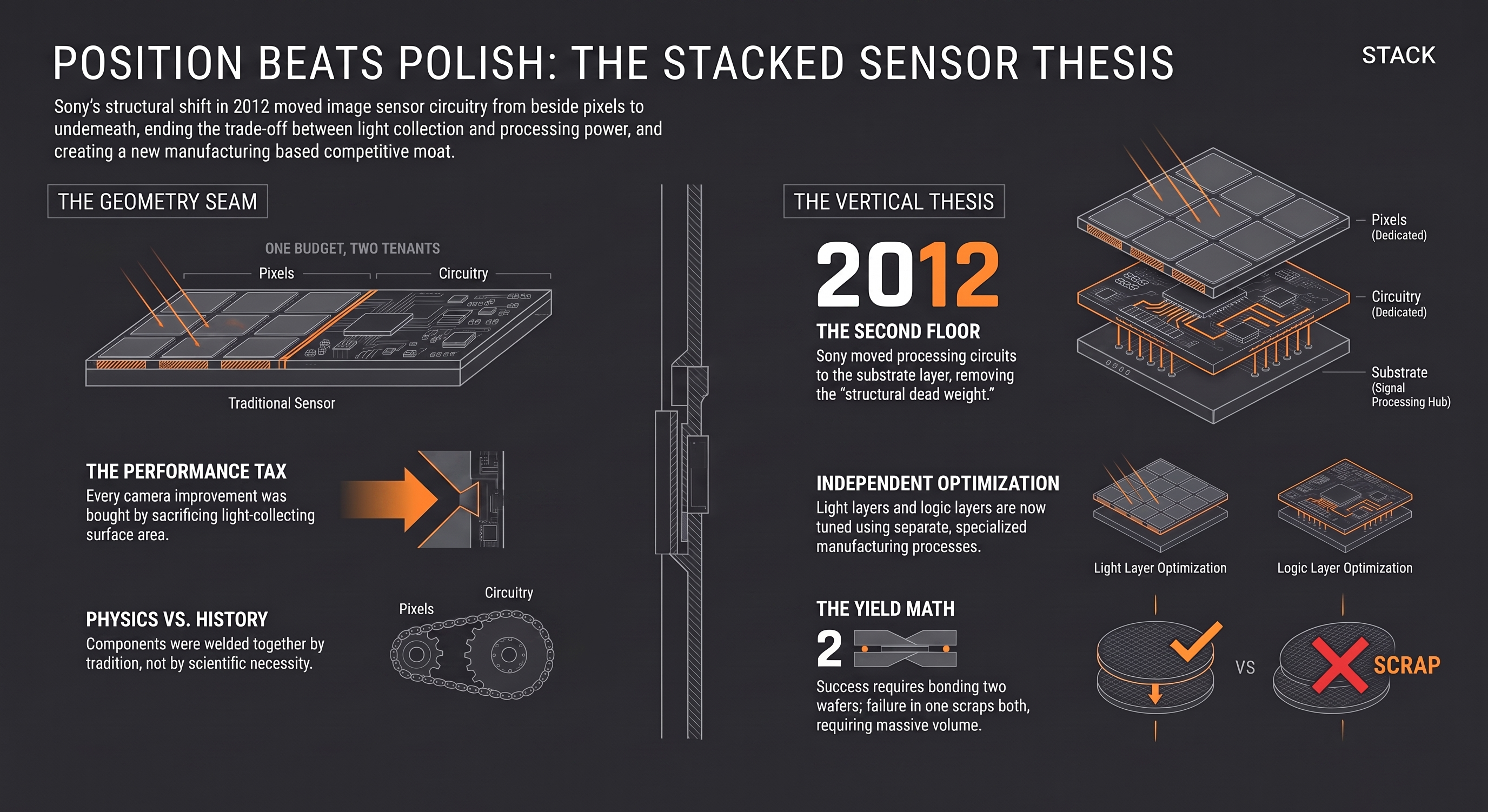 Download the one-page infographic
In the hyper-competitive arena of smartphone hardware, we have grown accustomed to a steady, rhythmic cadence of camera improvements. Every September, we are promised sharper images, faster capture speeds, and better performance in the dark, yet the physical footprint of the devices remains stubbornly the same. Most observers—and almost all of Sony’s competitors—assumed these gains were the result of "optimizing the pixel," a relentless, microscopic pursuit of better silicon chemistry. However, Sony’s stranglehold on this industry—providing over half of the world’s image sensors—was not won through chemistry. It was won through architecture. While the rest of the world was obsessed with the "what," Sony made a move that had almost nothing to do with cameras and everything to do with a wire. They realized that the greatest barrier to progress wasn't physics, but a crowded floor plan.
The Move to the Second Floor
In August 2012, Sony introduced a structural shift that would quietly redefine a trillion-dollar industry: the stacked image sensor. For decades, the anatomy of a sensor was strictly horizontal. The pixels, which collect light, and the circuits, which process the signal, sat side-by-side on the same flat surface. Sony decided to change the layout entirely. " They took the circuits out from beside the pixels and put them below. Same silicon, same physics, different floor plan. " By moving the signal processing to a subterranean level, Sony essentially added a second floor to the sensor. This wasn't a breakthrough in the fundamental nature of light collection; it was a spatial reorganization that ended a decades-old "budget war" between the eye and the brain of the device.
Turning Dead Weight into Brainpower
To understand the genius of this move, one must look at what was there before. In traditional chip manufacturing, the silicon layer beneath the functional components served a singular, humble purpose: structural support. It was a substrate, a passive slab designed to give the chip enough physical integrity to be handled. Sony’s breakthrough involved hollowing out this useless foundation and reimagining it as prime real estate. Instead of a passive support layer, they integrated the complex signal processing circuits directly into that space. As the shift took hold, "a slab whose only job was structural dead weight became the slab doing the work. " This transformation allowed the "eye" (the pixel layer) and the "brain" (the logic layer) to be optimized independently, turning a previously dormant component into the sensor's most functional asset.
The Geometry Seam and the End of Compromise
When components sit side-by-side on a single plane, they exist in a state of permanent negotiation. Every square micron allocated to a circuit is a square micron stolen from a pixel. This created a "geometry seam"—a hard limit where every improvement in logic required a sacrifice in light. In the source's evocative phrasing, it was "one budget, two tenants. "By stacking the layers, Sony stopped negotiating over that surface area. This separation allowed for a new level of specialization: the light-collecting layer could be built on a process tuned specifically for light, while the logic layer could be built on a process tuned for logic. These two functions had been "welded together for decades... not because anyone chose it, but because nobody had separated them. " Sony understood a fundamental truth of strategy: Position beats polish. By changing the geometry, they didn't just improve the product; they ended the compromise.
The Yield Math: A High-Stakes Gamble
This was not merely a design choice; it was a ruthless manufacturing bet. This is the unglamorous constraint under a decade of camera marketing: stacking requires bonding two separate wafers with millions of perfect connections. The scaling reality isn't physics—it’s yield math . In this architecture, the probability of success is the product of two separate probabilities. If one wafer is flawed, you scrap both. " A yield bet only pays back at volume. You need the units to absorb the pairs you scrap. " Because Sony owned over 50% of the market, they were the only player with the scale required to fund the scrap rate and master the process. This created a manufacturing moat that effectively decided who could even play in the smartphone market. That this was a "confirmed thesis" rather than a lucky break became clear in 2021. Sony repeated the move at a smaller scale, splitting the photodiode and the pixel transistors into their own separate layers. When a company repeats a structural decision at a deeper level, it isn't just a product cycle—it is a repeatable strategic framework.
The Portable Diagnostic: History vs. Physics
The Sony story offers a profound diagnostic for any leader or strategist. Sony succeeded because they identified a constraint that everyone else accepted as a law of nature and recognized it as a mere accident of history. They looked at the vertical space everyone else treated as "dead weight" and put it to work. To apply this logic to your own organization, you must look for the "welds"—areas where two functions are forced to share a single budget because "that’s how it’s always been. "
Is there one database serving both rights and analytics ?
Is there one service owning both authentication and sessions ? "Find the layer in your own system where two functions share one budget because nobody ever separated them. Ask whether they're welded by physics or only by history. " If the connection is merely historical, you have found your stacked sensor opportunity.
The Power of the Vertical
The most valuable decision Sony made was to stop running the same race as its competitors. While others were obsessed with the pixel itself, Sony looked at the vertical space beneath it. By reclaiming the "dead weight" of the substrate and mastering the brutal math of high-volume manufacturing, they moved from being a participant in the market to owning its infrastructure. The headline was a camera company getting better at cameras. The reality was a strategy company that mastered the vertical. As you evaluate your own systems, ask yourself: Where is your system currently paying a tax to history that physics no longer demands?